How to read an MCU datasheet (or hardware user guide for the MCU group)
This page is intended to be a very basic overview of how to navigate the datasheet for an MCU, which is typically a document of a thousand (or more!) pages. Some of the information on this page is general, and some applies specifically to the RA4M1 MCU group. To see a previous version of this document which focused on the Microchip SAM D21 (the MCU on the Arduino MKR1000), see here.
0: Useful links
- Arduino schematic
- RA1M1 Group Datasheet Summary
- RA4M1 Group User’s Manual: Hardware (“The Datasheet”) DATA/STORAGE WARNING: 1454 page PDF
- RA4M1 peripheral header files
Before reading this guide, review the lecture on Embedded Architectures, which contextualizes the hardware circuits that we are controlling using the registers defined in the datasheet.
Note: the datasheet uses the notation abcd 1234h to denote hexadecimal numbers. Class notes and code examples will use the C notation (e.g. 0xabcd1234, with or without spaces), instead. Binary numbers use the prefix 0b (e.g. 0b10110100) and decimal numbers use no prefix. You can review the meaning of hexadecimal/binary numbers and the conversion between them here.
1: Mapping Arduino pins to MCU pins
As we discussed in class, a Microcontroller (MCU) is a small computer that packages up a processor (CPU), I/O pins, and peripherals on a single piece of hardware. MCUs can be sold alone, or they can be part of a more complex electronics product, such as an Arduino. If we want to be able to directly program the MCU that is on the Arduino board instead of going through the functions provided by Arduino, we need to know how the MCU has been connected to the overall Arduino circuit (for example, the pins we use on the Arduino are physically wired to some of the MCU pins, so we might want to know the correspondence between names of Arduino pins and names of the MCU pins).
The MCU on the Arduino Uno WiFi R4 is in the Renesas RA4M1 family. As can be seen on the Arduino schematic, there are multiple components that make up an Arduino board, including the WiFi controller, the USB port, and the Arduino board pin headers. These all connect to different pins on the RA4M1. You can also see a “cartoon” version (block diagram) of the same schematic on page 8 of the Arduino datasheet (not to be confused with the MCU datasheet!):
To see which RA4M1 pins the Arduino board pins are connected to, you can look at the right side of the first page of the schematic, or page 18 of the Arduino datasheet:
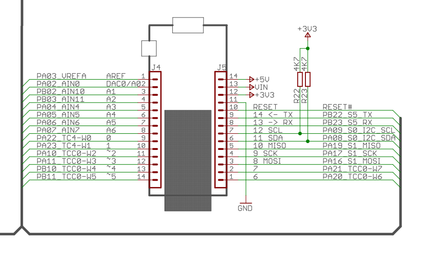
For example, GPIO Pin 1 (D1) of your Arduino is connected to pin name P302 on the RA4M1. Pins on the RA4M1 are arranged into groups, called Ports. The first digit of the pin name is the port number, and the second two digits are the pin number – port 3, pin 2, for our example.
2: Datasheet summary
If you want to quickly look up some facts about an MCU you are considering getting, the summary datasheet is the first place to look. The RA4M1 summary is here (131 page document). In this summary, among other things, you can see an overview of the peripherals (such as analog hardware, clocks, and serial communication capability) the MCU has, look up characteristics such as power and voltage ratings, and understand how the variants in the MCU family differ.
3: Full datasheet (also known as the Hardware User’s Manual)
While the summary is good for some information at-a-glance, MCUs are far too complicated to describe in a few dozen pages. More information about the MCU can be found in the full datasheet. The RA4M1 datasheet is here (warning: 1454 pages). Other names you might see for this document from other vendors are “family manual” or “family user’s guide.” This is a daunting document, so the overview you’re reading (and the labs in the course) are meant to guide you through navigating it to find the information you need.
A note on navigating the pdf: the file has embedded links (for example, in the table of contents) that will take you to specific chapters. Most PDF readers will also give you a way to navigate to specific chapters of the document using a sidebar (the Chrome pdf viewer, for example, calls it the “document outline”). We recommend having this sidebar open to easily navigate the document.
3.1: Registers
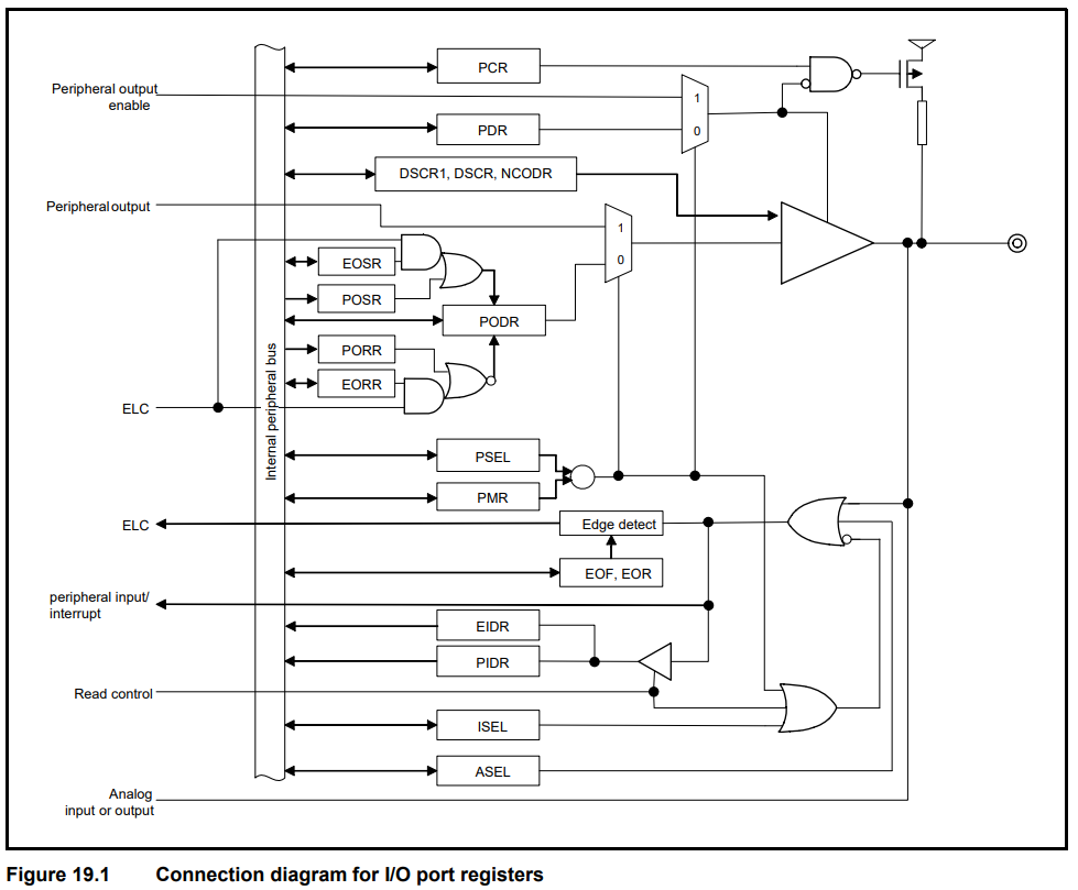
A register is a small piece of quickly-accessible, often volatile, memory. You can think of a register as an array of bits of a specific size – common register sizes include 8, 16, 32, and 64 bits. On a CPU, registers can be internal (available to the hardware only) or external (accessible by an assembly program) and are used for many things – keeping track of the program counter (control), storing the values of variables (data), or indicating that a previous operation had an arithmetic overflow (status), just to give a few examples. If you take computer architecture, you’ll learn much more about these sorts of registers! On an MCU, almost every peripheral is controlled by writing to MCU-specific registers. Here is a block diagram for the PORT peripheral, where the boxes named PCR, PDR, etc. are the MCU registers. Don’t spend time trying to decipher this diagram – all you need to take away from it is that the bits we write to the register are interpreted as physical electrical signals that “flip switches” in the hardware circuits on the MCU to configure what other signals get sent where. When we think of the datasheet as a manual for describing all of the possible configurations of these circuits for all of the available peripherals, we might start to understand why the datasheet is so large!
How do we know what bits to set in a given register? For every register that we can write to on our MCU, the datasheet provides a detailed register description. All of the bits of the register are labeled, and we’ll refer to named groups of the bits as “fields” (so in the diagram from 35.2.3 pictured below, ADST, ADCS, etc. are the fields of the ADCSR register):
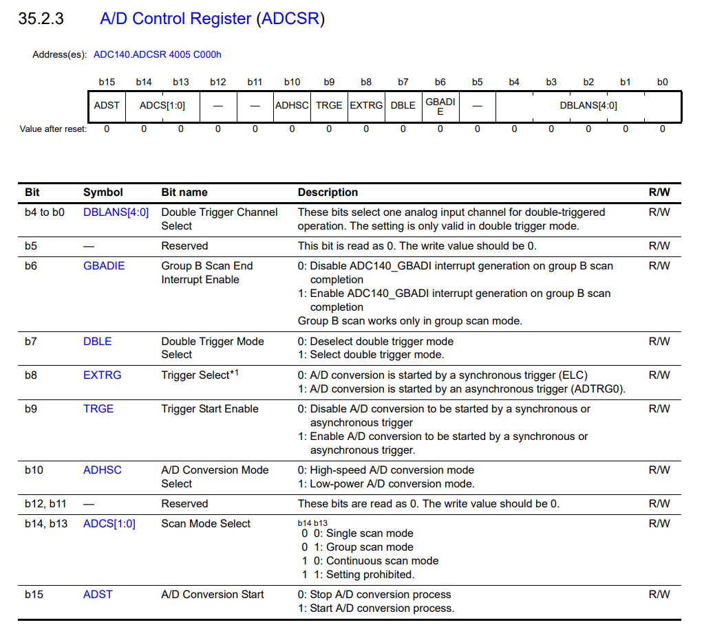
The table underneath each register gives a summary of how to set the values of specific fields for specific operation (for example, we can learn that bit 10 of the ADCSR register, which corresponds to the ADHSC field, switches between a high-speed Analog/Digital conversion mode when the value is 0, and a low-power A/D conversion more when the value is 1). Each field also has a detailed description lower down in the section.
Commonly, MCU registers are “memory-mapped” – in your code, the register address works just like any other memory address, and the hardware takes care of the routing of those addresses to the appropriate registers. While the Arduino API abstracts this idea away through pre-compilation and compilation, it is one of the core principles of explaining how we configure MCU hardware by writing software. Using the same concept, you can also read from some registers in your programs. The most common use cases are to read a signal from an input pin, and to check on which pin an interrupt occurred. Code that reads from and writes to MCU registers is explained at the bottom of this page.
3.2: Reading a peripheral chapter (PORT)
Using the Arduino API, we’ve learned to configure digital pins as input/output and read from/write to them using the functions pinMode, digitalWrite, and digitalRead. We’re learning that compilation and pre-compilation steps transform these functions into a set of writes to and reads from specific registers on the MCU. Most of these registers are called PORT registers, described in Chapter 19 of the datasheet.
The datasheet chapters that describe peripherals, such as PORT, include the following sections:
- An overview that describes what the peripherals can do
- Detailed descriptions of the registers, down to the bit level
- Operation, which describes the order in which registers must be written to and read from for common usages of the peripheral
- Usage notes to specify restrictions/special cases of writing to registers, such as interactions with other peripherals
It’s a good idea to read the first page of the overview, and then browse the operation section for the specific functionality you want, which will tell you which registers you are going to be reading/writing. Then, you can read the detailed description of these registers. We’ll see specific examples of this in class, and you’ll walk through this process a few times in the prelabs.
Even focusing on one peripheral section, it can be easy to get overwhelmed while trying to understand all of the functionality. Getting comfortable with this takes time (it’s taken Milda multiple MCUs and many, many hours). The prelabs are designed to guide you through one way of doing this – as you gain more practice, you’ll start to see patterns in the vocabulary and diagrams and it will become easier to find what you’re looking for or know what questions to ask. If you’re taking 1600, you’re more than likely seeing an MCU datasheet for the first time, so not having that practice may feel overwhelming or uncomfortable. You may encounter terms and abbreviations in the datasheet that you haven’t heard before, even in the sections we’re asking you to look. In the context of labs 3 and 4, we don’t need to know most of these terms, so we’ll simply ignore them. If you encounter something interesting in the datasheet and want to know why we’re ignoring it, go ahead and ask! Milda usually approaches datasheets by having a general sense of what she’s looking for (this is where the context and terminology from lectures, such as knowing what an interrupt is, can help) and then trying things out or looking up more information on terms that are unfamiliar.
In prelab 3, you’ll use the debugger to observe how the register values change when you call Arduino functions like pinMode. For lab 3 and the prelab, we’ll primarily use the PmnPFS register, but if you read the PORT register descriptions, you might see that the PORT registers give us several ways to specify the same configuration. For example, look at what the fields in the PCNTR1 register do, and then take a look at the PmnPFS register description to see if you can find how to modify the same settings in PmnPFS. If you read the field descriptions of the PCNTR1 register, you’ll see that the datasheet even says that the fields serve the same function as the corresponding PmnPFS fields. This means that you can change the field values in either register, and the effect on the hardware will be the same (and, in fact, a change in one register will be reflected in the other).
3.3: Clocks
While setting or reading (polling) a GPIO signal is typically not timing-dependent, most other peripherals depend on the clocks being configured correctly, because everything on an MCU happens in relation to a clock signal. Different MCUs require us to configure the clock(s) differently, and may provide multiple physical oscillators as sources for clock signals (electrical signals that look like square waves and allow circuits to be synchronized with each other by performing actions on the rising/falling edges of the wave). As described in Chapter 8, the RA4M1 has multiple on-chip oscillator sources (Table 8.1) with different frequencies and features, and multiple internal clock signals (Table 8.2) to control different peripherals. These clock signals are not necessarily independent – the register descriptions of SCKSCR (8.2.2) and SCKDIVCR (8.2.1) show that the same physical oscillator source is used for the system clock, peripheral module clocks, and flash interface clock. The MCU allows some flexibility here, in that SCKDIVCR lets the user select clock division ratios (for example, to make PCLKC run 4x slower than the system clock). However, when working with clocks on the Arduino Uno WiFi R4, we need to be careful not to reconfigure PCLKB, since the Arduino code is set up to use that clock for keeping track of system time (for functions like millis and delay). In prelab 4, we will delve deeper into the relationship between the on-chip oscillators, the clock circuits, and how the system clock and peripheral clocks are configured by the Arduino. We will also learn that some peripherals are able to further divide the signals from their respective clocks.
For now, our takeaway should be that tracking down the frequency at which any peripheral runs takes some sleuthing. For example, it might be that:
- The watchdog timer (WDT) is using PCLKB, but configured with a divider of 512 (so it is running at a frequency of PCKLB / 512)
- … but PCLKB itself is configured at 1/4 the speed of the system clock
- … and the system clock oscillator source is the HOCO (high-speed on-chip oscillator)
- … where the HOCO could be running at 24, 32, 48, or 64 MHz, depending on its configuration!
3.4: Pin multiplexing
Sometimes, a single pin on an MCU can be configured for different purposes (such as triggering an interrupt or connecting to the internal ADC). Since these different purposes require connecting the pin to different physical circuits, we have to have some way of telling the MCU which circuit to use. This is called multiplexing or pin function selection. For the RA4M1, the table in section 1.5 lists all of the possible functions pins may have. Not every pin can take on every possible function (since each function typically has a separate hardware circuit, this is basically a consequence of which pins are wired to which circuits). Table 1.7 shows which pins have which functions, and how to refer to that pin when configuring the corresponding peripheral. For example, we saw that PORT 302 was the GPIO “name” for what we know as Arduino digital pin 1. However, looking at page 72, that same physical pin can be used by the SPI peripheral, where it would be called SSLB3, so if we wanted to use that pin as part of the SPI peripheral, we would make sure that the SPI registers configure SSLB3 correctly. We would also configure this pin to go to the SPI peripheral (instead of being used as a GPIO pin) by setting the bits in the PmnPFS (19.2.5) register according to section 19.6. Prelab 3 will guide you through a specific example of pin multiplexing.
3.5: Interrupts
Remember that an MCU is made up of a CPU, I/O pins, and peripherals. In order for a peripheral to trigger an interrupt, there needs to be a special connection to the interrupt capabilities of the CPU, so that the CPU can execute the correct interrupt service routine. On the RA4M1, this connection is managed by the Interrupt Controller Unit (ICU), described in chapter 13. The RA4M1 allows us to connect up to 31 different events to the interrupt handler of the CPU (we can also detect interrupts and connect them to peripherals/handlers other than the CPU, such as the Direct Memory Access Controller, but we’ll focus on CPU interrupts for this class). This is done using the IELSRn register (section 13.2.6). Each possible event (think timer overflow, ADC conversion finishing, etc.) on the MCU has a unique numerical identifier (Table 13.4), which determines the value we put into the IELS bits of the IELSRn register to configure the interrupt. Besides configuring the MCU to make this connection, we would also write some code that configures the CPU interrupt at the correct priority level and the handler vector (the location of the code to execute when a specific interrupt occurs) in the NVIC (Nested Vector Interrupt Controller). Since the CPU on the RA4M1 is an Arm Cortex CPU, we will use NVIC functions provided by the Arm API (CMSIS) to do this in labs 3 and 4. In general, to configure an interrupt, we would:
- Configure the corresponding peripheral to generate an internal interrupt when something happens
- Connect the internal interrupt to the CPU using the IELSRn register
- Use the CMSIS functions
NVIC_SetVector,NVIC_SetPriority, andNVIC_EnableIRQto route execution to the handler function that contains the code we want to run when an interrupt happens
External interrupts (think button pushes) triggered by changes on GPIO pins get their own name (External Interrupt Request, or IRQ), and are configured using the IRQCRi (section 13.2.1) register. Determining which “i” (IRQ handler number) to configure is just another use of pin multiplexing, which we can look up in section 19.6. Note that the terminology here is a bit confusing – the 32 connections to the CPU interrupt controller are referred to as NVIC IRQs. They are called this because these interrupts are external to the CPU (even though they might be internal to the MCU, like a timer overflow). These are different from the 16 MCU IRQs (external interrupts), which the datasheet calls PORT IRQs. To configure a GPIO interrupt, we would perform one extra step to the general procedure above (the terminology in the steps has been refined to highlight the difference between NVIC IRQs and PORT IRQs):
- Configure the corresponding PORT pin as an input and set the appropriate PmnPFS bits to use the IRQ function of the pin
- Configure the MCU to detect a change on the pin as an interrupt (PORT IRQ) using the IRQCRi register
- Connect the MCU interrupt (PORT IRQ) to the CPU (NVIC IRQ) using the IELSRn register
- Use the CMSIS functions to connect the NVIC IRQ to the handler function that contains the code we want to run when an interrupt happens
3.6: Write protection and other register interactions
Sometimes, there might be restrictions on how registers must be written/read: the read-only bits of the register must be cleared before writing any other bits to it; or two registers cannot have conflicting values; or all of the bits of a register must be written to at once (more on this below). Often, this is described in the “Usage notes” section of each peripheral chapter. However, sometimes, even when you seem to follow all of the instructions, a peripheral isn’t working the way you want, or, when you pull up the debugger, the register values aren’t changing when you try to write to a register. Sometimes a hint as to why this is happening is given in the chapter in a non-obvious place, and other times you may have to actually do a search through the datasheet to see if any sections mention that the register or the peripheral is disabled in certain circumstances (ask Milda how she knows…). To make it a bit easier for you, we’ll let you know the non-obvious extra steps you’ll need to take to set the registers in labs 3 and 4. Scouring the datasheet for these takes some experience and intuition, so here are the non-obvious places we’ve learned to check in the RA4M1 datasheet, as examples of what to look for if you encounter a different datasheet:
- Chapter 12, on Register Write Protection, gives information on disabling the write protection for the registers that configure the clock generation circuit, low power modes, battery backup, and LVD (low voltage detect)
- The Module Stop Control Registers (MSTPCTRA-MSTPCTRD) in Chapter 10 describe the bits that must be set/cleared to enable/disable the peripherals on the MCU. Many of the peripherals are disabled by default when the device powers on. This chapter is also where you would configure specific peripherals as on/off for low-power mode.
- The Debug Stop Control Register (DBGSTOPCR) in section 2.6.4.2 enables/disables watchdog timer (WDT) operation when the device is in debugger mode. Because of the way the Arduino hardware is configured, connecting the Arduino to your computer via the USB cable puts the device in debugger mode, so the WDT won’t work unless we clear the correct bit in this register.
3.7: Putting it together: configuring a pin for ADC
We’ll talk about this in lecture on 9/18!
4: Option-setting memory
Writing to MCU registers allows you to configure the MCU while a program is running. What if we wanted to change the default configurations that the MCU uses? Some MCUs just come with default settings, and some MCUs have ways of configuring certain options or peripherals to desired states on a device reset. The RA4M1 uses a mix – you might have seen that each register description has a label of “value after reset” that shows what the registers look like on a hardware reset. However, some options, such as those for the independent watchdog timer (IWDT, not to be confused with WDT), cannot be configured while a program is running. Chapter 6, on option-setting memory, shows how specific default configurations are set at specific memory addresses (the technology of this memory is flash – why?). While it may be possible to write to this memory while a program is running (called self-programming), some peripherals are set up such that the memory is read directly after reset and at no other time, meaning that writes to those parts of option-setting memory will have no effect while the device is up and running. How, then, are these options set? In the same way that a program is loaded onto the device! A combination of hardware and software, called a “programmer,” copies code and data onto the device. On Arduino boards, the programmer circuit is built in to the USB connector circuit of the Arduino. For some MCUs, you might need to get a specific piece of hardware that the MCU gets inserted into in order to program it. In any case, a programmer for the RA4M1 is set up to write to option-setting memory.
Unfortunately for us, this is one of those things that the Arduino IDE obscures (as far as we understand from reading the Arduino repository, some default settings get loaded onto the Arduino, and to change these settings, we would have to change some configuration header files that say “generated configuration header file - do not edit” and then rebuild the Arduino source). However, since Renesas MCUs are also sold independently of Arduinos, Renesas provides its own programming tools, which allow you to write to the program-setting memory when programming the device (if curious, you can search for “project configuration editor” in the quick start guide to see screenshots of how you would do this in the tool – we suspect that these tools were used to generate the configuration header files). None of the things we need to do for labs 3 and 4 will require us to change the settings in option-setting memory, but the lab 4 writeup will ask you to interpret the values that are present at the option-setting memory locations and also to think through the implications of an MCU that has option-setting memory.
5: Writing code to configure the registers
You might have noticed that each register described in the datasheet has its own address. For example, the ADCSR register pictured earlier on this page is labeled with ADC140.ADCSR 4005 C000h, which means that the memory-mapped address for this register is 0x4005 C000. If we just had the datasheet available to us, we could write a program to write 0b10 to bits 13-14 (ADCS field) of this register (while keeping the other bits intact) using this information alone:
uint16_t* adcsr = 0x4005C000; // pointer to the address
uint16_t adcsr_val = *adcsr; // value at the address
adcsr_val = adcsr_val & ~(0b11 << 13); // clear bits 13, 14
adcsr_val = adcsr_val | (0b10 << 13); // write 10 to bits 13, 14
*adcsr = adcsr_val; // store back the value
(we could combine these into two lines or even one line of code if we wanted to).
However, this process tedious and prone to error. For a slightly less tedious approach, we can use the device-specific header provided by Renesas, which defines the locations and field offsets of all of the registers.
The header file is found here.
Documentation for the usage is found here. The important line is that “Each peripheral register set is provided as a struct. In general, the template to follow is: R_ + peripheral abbreviation + channel number + -> + register name [ + _b. + bitfield name]”. We also have access to macros of the bit positions of specific fields and bitmasks to isolate the bits in those fields. In the header file, we see that the ADCS field of the ACDSR register has the following macros:
 #define R_ADC0_ADCSR_ADCS_Pos              (13UL)      /*!< ADCS (Bit 13)                                         */
 #define R_ADC0_ADCSR_ADCS_Msk              (0x6000UL)  /*!< ADCS (Bitfield-Mask: 0x03)
The Pos macro gives the position (“rightmost,” or least significant) of the field, and the Msk macro “masks” off the bits (provides a value of 0 for all bit positions not in the field and 1 for all bit positions in the field, e.g. 0b00001110 for bits 1:3 in an 8-bit register). So, we could rewrite the code above as:
R_ADC0->ADCSR &= ~R_ADC0_ADCSR_ADCS_Msk; // clear bits 13, 14
R_ADC0->ADCSR |= 0b10 << R_ADC0_ADCSR_ADCS_Pos // write 10 to bits 13, 14
The Renesas documentation says that we can also access fields directly using the _b notation, which is useful when we want to modify just a single bitfield, replacing the lines above with:
R_ADC0->ADCSR_b.ADCS = 0b10;
However, this is inefficient (and sometimes incorrect!) when we want to modify multiple fields of a register at once (see the Bitfield Macros section of the Renesas documentation. In this case, we prefer using the Pos macros and bit-shifting to set the entire register at once, as in the R_GPT3 example in the Renesas documentation.
Some registers are arranged in groups, which we index into as we would arrays. It takes a bit of sleuthing to untangle the .h file here. For reference, the way we would use the PmnPFS PORT register is: R_PFS->PORT[PORT_NUM].PIN[PIN_NUM].PmnPFS. Why? Expand below to see how to figure that out from the .h file (don’t worry; in labs 3 and 4 we will just give you the notation).
Tracking the definitions in the .h file
This line defines R_PFS as having type R_PFS_Type *:
#define R_PFS ((R_PFS_Type *) R_PFS_BASE)
R_PFS_Type is a struct with a single field, PORT, which is a length-15 array of R_PFS_PORT_Types:
This explains why we access each PORT's PFS settings using the notation
typedef struct                         /*!< (@ 0x40040800) R_PFS Structure                                            */
{
    __IOM R_PFS_PORT_Type PORT[15];    /*!< (@ 0x00000000) Port [0..14]                                               */
} R_PFS_Type;
R_PFS->PORT[PORT_NUM]. If we look at how R_PFS_PORT_Type is defined, we see that it is a struct with a PIN field, which is an array of R_PFS_PORT_PIN_Type
The definition of
typedef struct
{
    __IOM R_PFS_PORT_PIN_Type PIN[16]; /*!< (@ 0x00000000) Pin Function Selects                                       */
} R_PFS_PORT_Type;
R_PFS_PORT_PIN_Type is a bit of a complicated combination of unions and structs, because the PmnPFS register can be accessed in 32-, 16-, or 8-byte units. For the 32-bit access, we can either access the whole register using R_PFS->PORT[PORT_NUM].PIN[PIN_NUM].PmnPFS, or we can use PmnPFS_b to access each individual field (a union just gives different ways to label and access data that exists at a single memory location -- it's different names for the same bits):
        union
        {
            __IOM uint32_t PmnPFS;        /*!< (@ 0x00000000) Pin Function Control Register                              */

            struct
            {
                __IOM uint32_t PODR  : 1; /*!< [0..0] Port Output Data                                                   */
                __IM uint32_t  PIDR  : 1; /*!< [1..1] Port Input Data                                                    */
                __IOM uint32_t PDR   : 1; /*!< [2..2] Port Direction                                                     */
                uint32_t             : 1;
                __IOM uint32_t PCR   : 1; /*!< [4..4] Pull-up Control                                                    */
                __IOM uint32_t PIM   : 1; /*!< [5..5] Port Input Mode Control                                            */
                __IOM uint32_t NCODR : 1; /*!< [6..6] N-Channel Open Drain Control                                       */
                uint32_t             : 3;
                __IOM uint32_t DSCR  : 2; /*!< [11..10] Drive Strength Control Register                                  */
                __IOM uint32_t EOFR  : 2; /*!< [13..12] Event on Falling/Rising                                          */
                __IOM uint32_t ISEL  : 1; /*!< [14..14] IRQ input enable                                                 */
                __IOM uint32_t ASEL  : 1; /*!< [15..15] Analog Input enable                                              */
                __IOM uint32_t PMR   : 1; /*!< [16..16] Port Mode Control                                                */
                uint32_t             : 7;
                __IOM uint32_t PSEL  : 5; /*!< [28..24] Port Function SelectThese bits select the peripheral
                                           *   function. For individual pin functions, see the MPC table                 */
                uint32_t : 3;
            } PmnPFS_b;
        };
6: A final note: what’s the point?
If you clicked around the Renesas documentation, you might have seen that it provides an API of functions that configure the MCU hardware. For example, instead of setting the ADCSR and other ADC registers by hand, as we did above, you could use the R_ADC_Open function to configure the ADC. The Renesas development tools include access to this API as part of the compilation process. The Arduino build chain also includes these functions (in fact, if you delve into the Arduino source code for built-in Arduino functions, you will see that the implementation makes use of them). Many MCU manufacturers provide this sort of API. This is a middle ground between the Arduino API and having to modify the registers directly. We can think of Arduino as packaging up embedded electronics and making them accessible without needing to know the deep specifics of embedded systems (for example, not needing to really know how an ADC works, but just wanting to read an analog signal in). The API that an MCU manufacturer provides serves a different purpose. If we’re programming an MCU directly (whether because it doesn’t come wrapped in a nice hobby package like Arduino, or because we want to optimize functionality not provided by the Arduino libraries), we can use our understanding of specific peripherals to make use of the MCU API.
Practically speaking, unless we really want ultra-fine control over our settings, we would probably opt for using the API most of the time, as this would save us time and be less error-prone. So why, then, are we fiddling with bits in registers? One answer is that understanding the datasheet helps you understand what the API functions are doing. Another is that some of you might need to decipher a datasheet for electronics you’re working with in your job or hobbies. Perhaps most honestly, this is one of those situations where taking a class is different than gaining experience “on the job.” Part of the purpose of CS1600 is to strip away some of the abstractions we’re used to working with in CS and really explore the connection between software and hardware. We want you to understand that, whenever you’re programming a computer (embedded or otherwise), some bits are physically being set in circuits that affect the routes that the electrons take through the wires. Actually manipulating those bits in those registers gets you as “close to the metal” as you can get with software. Plus, as you gain experience with these concepts, it starts to feel a little like becoming one with the esoteric magics of electronics. What’s cooler than knowing that the 1s and 0s you’re writing are affecting the flow of electricity? If you read to the end of this document, your reward is the knowledge that you’re on your way to becoming a wizard (if you simply skipped to the end and found this line, go back and read the full document, or it doesn’t count. Sorry, that’s the wizard rules 🧙).